Xenon (Motherboard): Difference between revisions
No edit summary |
|||
| Line 54: | Line 54: | ||
== Prototypes == | == Prototypes == | ||
There are 12 major prototypes of the | There are 12 major prototypes of the Xenon [[motherboard]]. The production board is the 11th version, Fab K, (-011). | ||
The following will describe typical or known build-ups, however build-ups will vary depending on [[ConfigID]]. | The following will describe typical or known build-ups, however build-ups will vary depending on [[ConfigID]]. | ||
Revision as of 15:38, 29 December 2024
 | |
| Part Number | X803600 |
|---|---|
| Introduced | Late 2005 |
| Used In | Xbox 360 (Original) |
| CPU Type | Waternoose |
| GPU Type | Y1 |
| CPU Process | 90nm |
| GPU Process | 90nm |
| eDRAM Process | 90nm |
| Nand Size | 16MB (Retail) 64MB (Dev) |
| Video Outputs | A/V |
| Wattage | 203W |
| 12V Amperage | 16.5A |
| Successor | Zephyr_A Elpis |
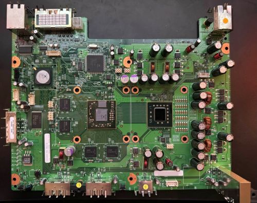
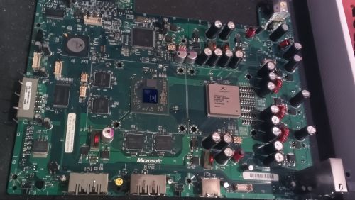
Xenon is the first motherboard and is used in the Original Xbox 360 series. The motherboard has a unique board layout compared to the later boards, especially noticeable with the capacitors around the CPU heatsink, and use of the ANA chip. The production board is known as Fab K, which is version -011.
Notes
- At some point in 2006, at least one of the manufacturers of the Xenon started applying glue around the CPU and GPU
- Some consoles use small yellow 820uF capacitors, while other consoles use silver 820uF solid capacitors
- Some capacitors used for voltage regulation positioned around the CPU heatsink are defective and prone to failure (see Capacitor Plague for details)
- There are two different versions of the XSB southbridge used, initially G0, and later switching to R0
- At some point in 2006, the extended GPU heatsink started being used on some systems instead of the low profile GPU heatsink
Specifications
- 90nm Waternoose DD2 or DD3 CPU
- 90nm Y1 GPU/eDRAM
- 512MB GDDR3 RAM
- 8x64MB Infineon/Qimonda HYB18H512321AF-13
- 8x64MB Samsung K4J52324QC-BC14
- XSB Southbridge
- ANA
- Nand
- 16MB Hynix HY27US08281A (Retail)
- 64MB Samsung K9F1208U0B (Dev)
- Boardcom or ICS Ethernet PHY
- Cypress Clock Generator
- Heatpipe CPU Heatsink
- GPU Heatsink
- Low Profile (Early/Mid Boards)
- Extended (Late Boards)
Variations
Elpis
Elpis is a modified Xenon used for refurbishing defective Xenon based systems. Major changes include use of the Elpis GPU and software differences.
Prototypes
There are 12 major prototypes of the Xenon motherboard. The production board is the 11th version, Fab K, (-011).
The following will describe typical or known build-ups, however build-ups will vary depending on ConfigID.
Fab A (-001)
First motherboard. Used with Willow and Alpha kits, with or without Shiva CPU. Typically has no GPU. Various Southbridge and ANA versions.
- Part Number: X801054-001
Fab B (-002)
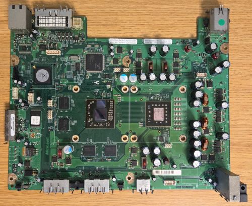
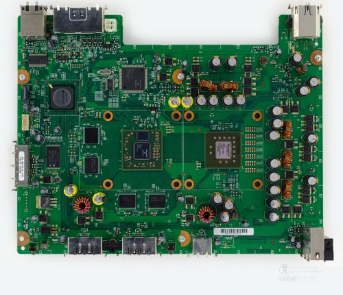
First fully working motherboard. Typically uses Shiva CPU and A11N1 or A11N2 GPU. Various Southbridge and ANA versions. Introduces optional Backup Clock Generator.
- Part Number: X801054-002
The following image has been upscaled for clarity:
Fab C (-003)
Not taped out. Reason not known.
- Part Number: X801054-003
Fab D (-004)
Updated Voltage Regulation. Little else is known.
- Part Number: X801054-004
Fab E (-005)
First motherboard to use Waternoose DD1 CPU out of the factory. Typically uses A11N2 GPU, E2 Southbridge, and B00 ANA. Removes Shiva support.
- Part Number: X801054-005
Fab F (-006)
Updated Voltage Regulation. Little else is known.
- Part Number: X801054-006
Fab G (-007)
The first PCB used for Beta refresh apart of the Partner program. Typically uses Waternoose DD1 CPU, A11N2 or A21N2 GPU, E2 or G0 Southbridge, and B00 ANA. Removes several Debug LEDs.
- Part Number: X801054-007
Fab H (-008)
First motherboard to use Waternoose DD2 CPU out of the factory. Typically uses A32 GPU. Uses G0 Southbridge and B02 ANA. Most CPUs are fused to 3.2GHz. Significant minor fixes.
- Part Number: X801054-008
Fab J (-009)
Part number changed to X803600. Uses Waternoose DD2 CPU, A32 GPU, G0 Southbridge, and B02 ANA. The CPU is fused to 2.8GHz or 3.2GHz. Fixed easily breakable IR sensor. Removes Titan support and almost all Debug LEDs. Adds additional but unused fan header. Most boards have an X-patch applied to fix a bug in GPU A32. Many 2.8GHz fused units were refurbished with 3.2GHz fused CPUs and used as Development Kits.
- Part Number: X803600-009
Fab J Prime (-010)
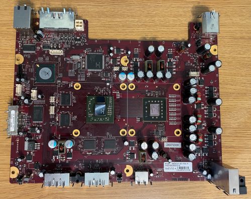
Derivative of Fab J, but 6-layer board. The PCB color is purple. Uses Waternoose DD2 CPU, A32 GPU, G0 Southbridge, and B02 ANA. The CPU is fused to 3.2GHz. The purpose of this board is unknown.
- Part Number: X803600-010
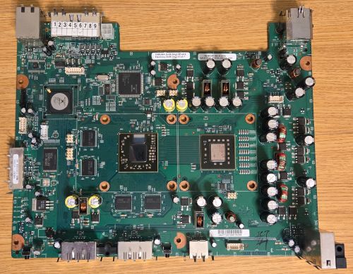
Fab K (-011)
The final motherboard. See Xenon (Motherboard) for details. Integrates the GPU A32 X-patch into the motherboard.
- Part Number: X803600-011
Fab M (-012)
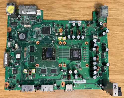
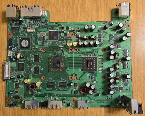
Only used internally. Some versions are 6-layer boards with top-side test-points added for POST_OUT. Otherwise, identical to Fab K.
- Part Number: X803600-012
The following image is a 4-layer Fab M without added test-points:
