Jasper: Difference between revisions
Jump to navigation
Jump to search
No edit summary |
No edit summary |
||
| Line 6: | Line 6: | ||
| type = Motherboard | | type = Motherboard | ||
| usedin = [[Xbox 360 (Original)]] | | usedin = [[Xbox 360 (Original)]] | ||
| cputype = [[ | | cputype = [[Loki]] | ||
| gputype = [[ | | gputype = [[Zeus]] | ||
| cpuprocess = 65nm | | cpuprocess = 65nm | ||
| gpuprocess = 65nm | | gpuprocess = 65nm | ||
| Line 24: | Line 24: | ||
[[File:X815842-002-Kronos.jpg|thumb|300px|upright|right|A July 2009 Jasper with a Kronos GPU]] | [[File:X815842-002-Kronos.jpg|thumb|300px|upright|right|A July 2009 Jasper with a Kronos GPU]] | ||
* The 80nm [[ | * The 80nm [[Rhea]] GPU has been replaced with the 65nm [[Zeus]] GPU | ||
* [[Hynix RAM#H5RS5223CFR-14C|Hynix H5RS5223CFR-14C]] and [[Hynix RAM#H5RS1H23MFR-14C|Hynix H5RS1H23MFR-14C]] RAM were added as options | * [[Hynix RAM#H5RS5223CFR-14C|Hynix H5RS5223CFR-14C]] and [[Hynix RAM#H5RS1H23MFR-14C|Hynix H5RS1H23MFR-14C]] RAM were added as options | ||
* The [[XSB]] has been replaced with the [[PSB]] | * The [[XSB]] has been replaced with the [[PSB]] | ||
| Line 35: | Line 35: | ||
=== Specifications === | === Specifications === | ||
* 65nm IBM [[ | * 65nm IBM [[Loki]] CPU | ||
* 65nm ATi [[ | * 65nm ATi [[Zeus]] GPU with integrated 80nm NEC [[eDRAM]] | ||
* 512MB GDDR3 RAM | * 512MB GDDR3 RAM | ||
** 8x64MB [[Hynix RAM#H5RS5223CFR-14C|Hynix H5RS5223CFR-14C]] | ** 8x64MB [[Hynix RAM#H5RS5223CFR-14C|Hynix H5RS5223CFR-14C]] | ||
Revision as of 12:21, 19 January 2023
 | |
| Part Number | X815842 |
|---|---|
| Introduced | Late 2008 |
| Type | Motherboard |
| Used In | Xbox 360 (Original) |
| CPU Type | Loki |
| GPU Type | Zeus |
| CPU Process | 65nm |
| GPU Process | 65nm |
| eDRAM Process | 80nm |
| Nand Size | 16MB, 256MB, 512MB |
| Video Outputs | A/V and HDMI |
| Wattage | 150W |
| 12V Amperage | 12.1A |
| Predecessor | Falcon |
| Successor | Tonasket |
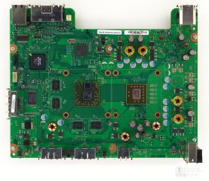
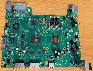
Jasper is the successor to the Falcon and is used in the Original Xbox 360 series.
Notable Differences
- The 80nm Rhea GPU has been replaced with the 65nm Zeus GPU
- Hynix H5RS5223CFR-14C and Hynix H5RS1H23MFR-14C RAM were added as options
- The XSB has been replaced with the PSB
- Arcade Jaspers came with 256MB (later 512MB) nand chips that combine system storage and a Memory Unit
- Traces and pads for an additional flash controller (referred to as "DUMBO" or "PANDA") have been added, but never populated
- Other small changes were made to the board layout
- Very late Jaspers manufactured in July 2009 come with the Kronos GPU instead of the Zeus GPU
- Some boards use solid state capacitors for the CPU and GPU output filters
- Some of the boards no longer have glue applied around the CPU and GPU
Specifications
- 65nm IBM Loki CPU
- 65nm ATi Zeus GPU with integrated 80nm NEC eDRAM
- 512MB GDDR3 RAM
- 8x64MB Hynix H5RS5223CFR-14C
- 4x128MB Hynix H5RS1H23MFR-14C
- 4x128MB Qimonda HYB18H1G321AF-14
- PSB Southbridge
- HANA
- Nand
- 16MB Hynix HY27US08281A
- 256MB Hynix HY27UF082G2B
- 512MB Hynix HY27UF084G2B
- 512MB Samsung K9F4G08U0B
- Boardcom or ICS Ethernet PHY
- Aluminum CPU Heatsink
- Extended GPU Heatsink
Variations
Tonasket
Tonasket is a minor revision of Jasper. Major changes include use of the Kronos GPU and board layout cleanup.
