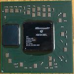
GPU
 The original GPU, Y1 | |
| Introduced | Late 2005 |
|---|---|
| Designed By | ATi Microsoft NEC (eDRAM) |
| Codename | Xenos (90nm) Gunga (65nm) |
| Type | GPU |
| Used In | Original Xbox 360 |
| Clock Speed | 500MHz |
| Memory | 10MB eDRAM |
| Successor | XCGPU |
The GPU, codename Xenos (later Gunga) is the graphics processor, northbridge, and memory controller used in the Xbox 360. It also contained an eDRAM daughter die that contains additional logic.
The processor was developed by Microsoft and ATi, and the first version was codenamed Y1, which stands for Year 1. The eDRAM was designed by NEC. Microsoft would later take over development of both dies with Gunga and Styx
Chip Matrix
The GPU is the parent die (P-die) while the eDRAM is the daughter die (D-die).
| Chip | P-Die | D-Die |
|---|---|---|
| Y1 | Xenos C1 (90nm) | Edifis (90nm) |
| Y2 | Xenos C2 (90nm) | Edifis (90nm) |
| Rhea | Xenos C2 (90nm) | Styx-90 (90nm) |
| Elpis | Xenos C2 (90nm) | Styx-90 (90nm) |
| Zeus | Gunga (65nm) | Styx-90 (90nm) |
| Kronos | Gunga (65nm) | Styx-65 (65nm) |
| Vejle | Vejle (45nm) | Styx-65 (65nm) |
| Oban | Oban (32nm) | |
Chip Variants
Y1 (90nm)
The initial version, Y1, entered production in 2005 and is used on the Xenon and Zephyr_A motherboards. Initial versions were defective while later versions became reliable. It uses the Edifis eDRAM.
Y2 (90nm)
In 2007, the GPU was revised and the physical size of the die reduced. The process remained at 90nm and the eDRAM remained unchanged. Y2 is used on the Zephyr_B motherboard.
Rhea (90nm)
Later in 2007, The Y2 version was revised with the Styx-90 eDRAM. Named Rhea, it is used on the Zephyr_C and Falcon motherboards. Later versions of the chip were the first chips installed on newly produced consoles to be reliable. Multiple versions of Rhea were created as Microsoft experimentated during the attempts to make the chip reliable.
Elpis (90nm)
In 2009, fixed 90nm chips stopped being produced, however Microsoft still had Xenons to repair and refurbish. Since the fixed Rhea chip was still being produced, Microsoft chose to slightly modify it in order to allow a revised chip to be retrofitted in place of a defective one. This modification to Xenon boards was named Elpis, which served as the name of the GPU and the motherboard with this GPU installed.
Zeus (65nm)
In 2008, the chip was redesigned for the 65nm process under the codename Gunga. It still uses the Styx-90 eDRAM. Named Zeus, it is used on the Jasper motherboard. It is the first chip where all variants are reliable.
Kronos (65nm)
In 2009, the Zeus chip was revised with a Styx-65 eDRAM. Named Kronos, it is used on the Jasper (July 2009 only) and Tonasket motherboards.
XCGPU
In 2010, the XCPU was combined with the GPU to create a system-on-a-chip, called the XCGPU.
GPU Specifications
- 500Mhz clock speed
- 48 floating-point vector processors divided into 3 dynamically scheduled SIMD groups (16 each)
- Unified shader architecture
- 16 texture addressing units
- 16 texture filtering units
- 8 pixel rendering pipelines
- Direct access to CPU L2 cache
GPU Variants
Xenos C1
Xenos C1 is the first GPU die and was designed by ATi. It was manufactured on the 90nm process and was used in the Y1 GPU.
Xenos C2
Xenos C2 is the cost-reduced version of Xenos C1. It is still manufactured on the 90nm process but has a smaller physical size.
Gunga
Gunga is the redesigned GPU die for the 65nm process. The design was done by Microsoft, not ATi. It is used on Zeus and Kronos.
Vejle
Vejle is the first CGPU die which integrates the XCPU and GPU. The process was shrunk to 45nm. It shares the name with the Vejle CGPU.
Oban
The Oban CGPU integrates Vejle with Styx-65. The process was shrunk to 32nm. It shares the name with the Oban CGPU.
eDRAM Specifications
- 10MB 256GB/s eDRAM
- Contains logic for:
- 4-sample anti-aliasing
- Alpha compositing
- Color
- Z/stencil buffering
eDRAM Variants
Edifis
Edifis is the first eDRAM die used on the GPU and was designed by NEC. It was only manufactured on the 90nm process. It is used on the Y1 and Y2 GPUs.
Styx
Styx is the redesigned eDRAM die and replaces Edifis. The redesign was done by Microsoft, not NEC.
Styx-90
Styx-90 is the first version of Styx and is manufactured on the 90nm process. It is used on all versions of Rhea, Elpis, and Zeus.
Styx-65
Styx-65 is a die shrink of Styx-90 to the 65nm process. It is used on Kronos and the Vejle XCGPU.
Oban
The Oban CGPU integrates Vejle with Styx-65. As a result, there is no daughter die anymore.