Jasper: Difference between revisions
No edit summary |
|||
| (31 intermediate revisions by 2 users not shown) | |||
| Line 9: | Line 9: | ||
| cpuprocess = 65nm | | cpuprocess = 65nm | ||
| gpuprocess = 65nm | | gpuprocess = 65nm | ||
| edramprocess = | | edramprocess = 90nm | ||
| nandsize = 16MB, 256MB, 512MB | | nandsize = 16MB, 256MB, 512MB | ||
| video = [[A/V]] and HDMI | | video = [[A/V]] and HDMI | ||
| Line 18: | Line 18: | ||
}} | }} | ||
'''Jasper''' is the successor to the [[Falcon]] [[motherboard]] and is used in the [[Original Xbox 360]] series. | '''Jasper''' is the successor to the [[Falcon]] [[motherboard]] and is used in the [[Original Xbox 360]] series. The production board is known as [[#Jasper_A1|Jasper_A1]]. | ||
=== Notable Differences === | === Notable Differences === | ||
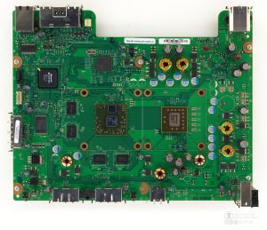
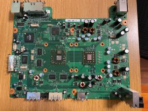
[[File:X815842-002-Kronos.jpg|thumb|300px|upright|right|A July 2009 | [[File:X815842-002-Kronos.jpg|thumb|300px|upright|right|A July 2009 Jasper_A1 with a Kronos GPU]] | ||
* The | * The [[Rhea]] GPU has been replaced with the [[Zeus]] GPU | ||
* [[Hynix RAM#H5RS5223CFR-14C|Hynix H5RS5223CFR-14C]] and [[Hynix RAM#H5RS1H23MFR-14C|Hynix H5RS1H23MFR-14C]] RAM were added as options | * [[Hynix RAM#H5RS5223CFR-14C|Hynix H5RS5223CFR-14C]] and [[Hynix RAM#H5RS1H23MFR-14C|Hynix H5RS1H23MFR-14C]] RAM were added as options | ||
* The [[XSB]] Southbridge has been replaced with the [[PSB]] Southbridge | * The [[XSB]] Southbridge has been replaced with the [[PSB]] Southbridge | ||
* [[Arcade]] Jaspers came with 256MB (later 512MB) nand chips that combine system storage and a [[Memory Unit]] | * [[Arcade]] Jaspers came with 256MB (later 512MB) nand chips that combine system storage and a [[Memory Unit]] | ||
* Traces and pads for an additional flash controller (referred to as "DUMBO" or "PANDA") have been added, but never populated | * Traces and pads for an additional flash controller (referred to as "DUMBO" or "PANDA") have been added, but never populated | ||
* Very late Jaspers manufactured in July 2009 come with the [[Kronos]] GPU instead of the [[Zeus]] GPU | |||
* Very late Jaspers manufactured in July 2009 come with the [[ | |||
* Some boards use solid state capacitors for the CPU and GPU output filters | * Some boards use solid state capacitors for the CPU and GPU output filters | ||
* Some of the boards no longer have glue applied around the CPU and GPU | * Some of the boards no longer have glue applied around the CPU and GPU | ||
=== Specifications === | === Specifications === | ||
* 65nm | * 65nm [[Loki]] CPU | ||
* 65nm | * GPU | ||
** 65nm [[Zeus]] GPU with 90nm eDRAM (Before July 2009) | |||
** 65nm [[Kronos]] GPU with 65nm eDRAM (July 2009) | |||
* 512MB GDDR3 RAM | * 512MB GDDR3 RAM | ||
** 8x64MB [[Hynix RAM#H5RS5223CFR-14C|Hynix H5RS5223CFR-14C]] | ** 8x64MB [[Hynix RAM#H5RS5223CFR-14C|Hynix H5RS5223CFR-14C]] | ||
| Line 47: | Line 48: | ||
** 512MB [[Nand#Hynix HY27UF084G2B|Hynix HY27UF084G2B]] | ** 512MB [[Nand#Hynix HY27UF084G2B|Hynix HY27UF084G2B]] | ||
** 512MB [[Nand#Samsung K9F4G08U0B|Samsung K9F4G08U0B]] | ** 512MB [[Nand#Samsung K9F4G08U0B|Samsung K9F4G08U0B]] | ||
* Boardcom or ICS Ethernet PHY | * Boardcom or ICS [[Ethernet PHY]] | ||
* [[Heatsink#Aluminum CPU|Aluminum]] CPU Heatsink | * [[Heatsink#Aluminum CPU|Aluminum]] CPU Heatsink | ||
* [[Heatsink#Extended GPU|Extended]] GPU Heatsink | * [[Heatsink#Extended GPU|Extended]] GPU Heatsink | ||
== Variations == | == Variations == | ||
=== Jasper_A0 === | |||
First Jasper version, uses the [[XSB]] southbridge. Only used for EV, never used in production [[retail]] units. | |||
=== Jasper_A1 === | |||
Same as [[#Jasper_A0|Jasper_A0]], but with the [[PSB]] southbridge. This is the version that was used in production. | |||
=== Advanced === | |||
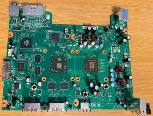
[[File:X817861-002.jpg|thumb|300px|upright|right|An Advanced board with the Zeus GPU]] | |||
Advanced, or Jasper Advanced, is a slightly modified [[Jasper#Jasper A1|Jasper_A1]] for the [[XDK-GB|Xbox 360-GB Development Console]] and its [[Prototype XDK-GB|prototypes]]. Support for 1GB of [[RAM]] was added by routing the 13th addressing line. Other minor changes and cleanup were made. Early versions use the [[Zeus]] GPU, while later boards used [[Kronos]]. | |||
=== Tonasket === | === Tonasket === | ||
{{Main|Tonasket}} | {{Main|Tonasket}} | ||
[[Tonasket]], initially known as Jasper_B, is a revision of Jasper. Changes include use of the [[Kronos]] GPU and board layout cleanup. | |||
{{Console Components}} | {{Console Components}} | ||
[[Category:Motherboards]] | [[Category:Motherboards]] | ||
Latest revision as of 01:54, 16 May 2024
 | |
| Part Number | X815842 |
|---|---|
| Introduced | Late 2008 |
| Used In | Xbox 360 (Original) |
| CPU Type | Loki |
| GPU Type | Zeus |
| CPU Process | 65nm |
| GPU Process | 65nm |
| eDRAM Process | 90nm |
| Nand Size | 16MB, 256MB, 512MB |
| Video Outputs | A/V and HDMI |
| Wattage | 150W |
| 12V Amperage | 12.1A |
| Predecessor | Falcon |
| Successor | Tonasket |
Jasper is the successor to the Falcon motherboard and is used in the Original Xbox 360 series. The production board is known as Jasper_A1.
Notable Differences
- The Rhea GPU has been replaced with the Zeus GPU
- Hynix H5RS5223CFR-14C and Hynix H5RS1H23MFR-14C RAM were added as options
- The XSB Southbridge has been replaced with the PSB Southbridge
- Arcade Jaspers came with 256MB (later 512MB) nand chips that combine system storage and a Memory Unit
- Traces and pads for an additional flash controller (referred to as "DUMBO" or "PANDA") have been added, but never populated
- Very late Jaspers manufactured in July 2009 come with the Kronos GPU instead of the Zeus GPU
- Some boards use solid state capacitors for the CPU and GPU output filters
- Some of the boards no longer have glue applied around the CPU and GPU
Specifications
- 65nm Loki CPU
- GPU
- 512MB GDDR3 RAM
- 8x64MB Hynix H5RS5223CFR-14C
- 4x128MB Hynix H5RS1H23MFR-14C
- 4x128MB Qimonda HYB18H1G321AF-14
- PSB Southbridge
- HANA
- Nand
- 16MB Hynix HY27US08281A
- 256MB Hynix HY27UF082G2B
- 512MB Hynix HY27UF084G2B
- 512MB Samsung K9F4G08U0B
- Boardcom or ICS Ethernet PHY
- Aluminum CPU Heatsink
- Extended GPU Heatsink
Variations
Jasper_A0
First Jasper version, uses the XSB southbridge. Only used for EV, never used in production retail units.
Jasper_A1
Same as Jasper_A0, but with the PSB southbridge. This is the version that was used in production.
Advanced
Advanced, or Jasper Advanced, is a slightly modified Jasper_A1 for the Xbox 360-GB Development Console and its prototypes. Support for 1GB of RAM was added by routing the 13th addressing line. Other minor changes and cleanup were made. Early versions use the Zeus GPU, while later boards used Kronos.
Tonasket
Tonasket, initially known as Jasper_B, is a revision of Jasper. Changes include use of the Kronos GPU and board layout cleanup.

