Vejle: Difference between revisions
Jump to navigation
Jump to search
No edit summary |
|||
| Line 24: | Line 24: | ||
}} | }} | ||
'''Valhalla''' (also known as '''Vejle''') is the first [[XCGPU]] and is used on the [[Trinity]], [[Corona]], [[Waitsburg]], and [[Stingray]] motherboards. It is the successor to [[Loki]] CPU and [[Kronos]] GPU and is manufactured on the 45nm process (except for the [[eDRAM]] daughter-die, which still used [[Styx-65 | '''Valhalla''' (also known as '''Vejle''') is the first [[XCGPU]] and is used on the [[Trinity]], [[Corona]], [[Waitsburg]], and [[Stingray]] motherboards. It is the successor to [[Loki]] CPU and [[Kronos]] GPU and is manufactured on the 45nm process (except for the [[eDRAM]] daughter-die, which still used [[Styx]]-65). Valhalla adds an [[IHS|integrated heat spreader]] over the dies. | ||
== Specifications == | == Specifications == | ||
Revision as of 04:29, 5 April 2024
 Valhalla | |
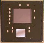 Valhalla with IHS removed | |
| Part Number | X818337 |
|---|---|
| Introduced | Mid 2010 |
| Designed By | ATi IBM Microsoft NEC (eDRAM) |
| Type | XCGPU |
| Used In | Trinity Corona Waitsburg Stingray |
| Clock Speed | 3.2GHz (CPU) 500MHz (GPU) |
| Cache | L1: 32KB/32KB (CPU) L2: 1MB (CPU) |
| Memory | 10MB eDRAM (GPU) |
| Instruction Set | PowerPC RISC (CPU) |
| Cores | 3 (CPU) |
| Threads | 6 (CPU) |
| Process | 45nm (CGPU die) 65nm (eDRAM die) |
| Package | Flip-chip BGA1155 |
| Predecessor | Loki Kronos |
| Successor | Oban |
Valhalla (also known as Vejle) is the first XCGPU and is used on the Trinity, Corona, Waitsburg, and Stingray motherboards. It is the successor to Loki CPU and Kronos GPU and is manufactured on the 45nm process (except for the eDRAM daughter-die, which still used Styx-65). Valhalla adds an integrated heat spreader over the dies.
Specifications
CPU
- 3 two-way SMD-capable RISC cores clocked at 3.2GHz
- SIMD: Two VMX128 units
- 32KB L1 data cache
- 32KB L1 instruction cache
- 1MB L2 cache at 1.6 GHz with a 256-bit bus
- 21.6GB/s FSB
- 768 bits of IBM eFUSE One-Time-Program memory for fusesets
- One-Time-Programmable ROM and 64KB SRAM for the 1BL and Config Ring
- Big-endian architecture
- A02 stepping
- 45nm process
GPU
- 500Mhz clock speed
- 48 floating-point vector processors divided into 3 dynamically scheduled SIMD groups (16 each)
- Unified shader architecture
- 16 texture addressing units
- 16 texture filtering units
- 8 pixel rendering pipelines
- Direct access to CPU L2 cache
- A02 stepping
- 45nm process
eDRAM (Styx-65)
- 10MB 256GB/s eDRAM
- Contains logic for:
- 4-sample anti-aliasing
- Alpha compositing
- Color
- Z/stencil buffering
- GS21 stepping
- 65nm process
Details
Valhalla uses the Styx-65 eDRAM.
- Part Number: X818337
Prototypes
Engineering Samples by stepping.
A00
First version.
- Part Number: Unknown
A01
Minor update.
- Part Number: X850448-001
A02
Minor update. Engineering sample for the final production chip.
- Part Number: Unknown
