Elpis (GPU): Difference between revisions
Jump to navigation
Jump to search
No edit summary |
No edit summary |
||
| Line 6: | Line 6: | ||
| introduced = Mid 2009 | | introduced = Mid 2009 | ||
| designedby = ATi<br>Microsoft<br>NEC (eDRAM) | | designedby = ATi<br>Microsoft<br>NEC (eDRAM) | ||
| codename = | | codename = Elpis | ||
| type = [[GPU]] | | type = [[GPU]] | ||
| usedin = [[Elpis (Motherboard)]] | | usedin = [[Elpis (Motherboard)]] | ||
Revision as of 17:32, 16 June 2023
 | |
| Part Number | X819195 |
|---|---|
| Introduced | Mid 2009 |
| Designed By | ATi Microsoft NEC (eDRAM) |
| Codename | Elpis |
| Type | GPU |
| Used In | Elpis (Motherboard) |
| Clock Speed | 500MHz |
| Memory | 10MB eDRAM |
| Process | 80nm (Both dies) |
| Package | Flip-chip BGA1017 |
| Predecessor | Y1 |
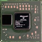
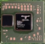
Elpis is an 80nm GPU specifically made for retrofitting faulty Xenon motherboards. Once retrofitted, the motherboard is referred to as Elpis (Motherboard). The Elpis GPU was created by slightly modifying the fixed (higher Tg) version of the Rhea GPU.
Specifications
GPU
- 500Mhz clock speed
- 48 floating-point vector processors divided into 3 dynamically scheduled SIMD groups (16 each)
- Unified shader architecture
- 16 texture addressing units
- 16 texture filtering units
- 8 pixel rendering pipelines
- Direct access to CPU L2 cache
- B14L stepping
- 80nm process
eDRAM
- 10MB 256GB/s eDRAM
- Contains logic for:
- 4-sample anti-aliasing
- Alpha compositing
- Color
- Z/stencil buffering
- FS21 stepping
- 80nm process
Details
The only known change from Rhea to create Elpis was swizzling (flipping) the PCIe balls on the chip in order to match the ballout of the original 90nm Y1 chip it replaces. Like Rhea, it uses the Styx eDRAM. These chips are known to be reliable.
- Part Number: X819195
