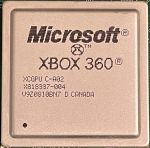
XCGPU
 The original XCGPU, Valhalla | |
| Introduced | Mid 2010 |
|---|---|
| Designed By | ATi IBM Microsoft NEC (eDRAM) |
| Type | SoC |
| Used In | Xbox 360 S Xbox 360 E |
| Clock Speed | 3.2GHz (CPU) 500MHz (GPU) |
| Cache | L1: 32KB/32KB (CPU) L2: 1MB (CPU) |
| Memory | 10MB eDRAM (GPU) |
| Instruction Set | PowerPC RISC (CPU) |
| Cores | 3 (CPU) |
| Threads | 6 (CPU) |
| Predecessor | XCPU Xenos |
The Microsoft XCGPU, codenamed Valhalla, is a combination of the XCPU and Xenos GPU. It was created in order to reduce the size and complexity of the motherboard for the Xbox 360 S. The XCGPU is the first high performance integrated system-on-a-chip. The XCGPU contains an "emulated" FSB between the CPU and GPU areas of the die. This ensures that latencies are the same, making the XCGPU perform as close as possible to the previous separate CPU and GPU.
The XCGPU was developed by Microsoft and IBM.
Specifications
CPU
- 3 two-way SMD-capable RISC cores clocked at 3.2GHz
- SIMD: Two VMX128 units
- 32KB L1 data cache
- 32KB L1 instruction cache
- 1MB L2 cache at 1.6 GHz with a 256-bit bus
- 21.6GB/s FSB
- 768 bits of IBM eFUSE One-Time-Program memory for fusesets
- One-Time-Programmable ROM and 64KB SRAM for the 1BL and Config Ring
- Big-endian architecture
GPU
- 500Mhz clock speed
- 48 floating-point vector processors divided into 3 dynamically scheduled SIMD groups (16 each)
- Unified shader architecture
- 16 texture addressing units
- 16 texture filtering units
- 8 pixel rendering pipelines
- Direct access to CPU L2 cache
eDRAM
- 10MB 256GB/s eDRAM
- Contains logic for:
- 4-sample anti-aliasing
- Alpha compositing
- Color
- Z/stencil buffering
Variants
Valhalla (45nm)
In 2010, the XCPU was shrunk to the 45nm process and combined with the Xenos graphics chip to create a system-on-a-chip, called the XCGPU. The eDRAM remains on a separate die and an IHS was added. Codename Valhalla, it is used on the Trinity and Corona motherboards.
Winchester CGPU
In 2014, the XCGPU process was shrunk by an unknown amount and the eDRAM die was integrated into the CGPU die. The codename and specifics for this chip are unknown. The single die design meant that the IHS was no longer needed. It is used on the Winchester motherboard and is notable for patching the RGH exploit.