ANA: Difference between revisions
Jump to navigation
Jump to search
No edit summary |
|||
| Line 31: | Line 31: | ||
=== B00 === | === B00 === | ||
[[File:X02014-002-Early.jpg|150px]] | |||
[[File:X02014-002.jpg|150px]] | [[File:X02014-002.jpg|150px]] | ||
Latest revision as of 00:33, 2 August 2024
 | |
| Introduced | Late 2005 |
|---|---|
| Designed By | Microsoft |
| Used In | Xenon Elpis |
| Process | 180nm |
| TDP | 1.3W |
| Package | LQFP144 |
| Successor | HANA |
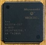
The ANA is the analog chip used on the Xenon motherboard. It contains the video encoders, DACs, clock generators (unused), thermal sensor circuits, fan driver op-amps, and some of the Power On Reset logic.
The chip was developed by Microsoft.
Specifications
- Digital video encoder with 4 DACs
- 5 thermal diode channels
- 2 fan driver op-amps
- Power on reset logic cell
- Clock synthesizer:
- 4x 100MHz differential: CPU, GPU, PCIe, SATA
- 1x 48MHz single ended: SMC, USB
- 2x 25MHz single ended: Ethernet, SATA
- 1x 24.576MHz single ended: Audio
- 2x programmable clocks: DVE video, Pixel
- B03 stepping
- 180nm process
- 1.3W TDP
Details
The clock generators on the ANA are not used due to excessive PLL jitter. The Backup Clock Generator is used instead to generate system clocks. ANA still generates the video and audio clocks. The PLL jitter issue was fixed in HANA.
- Part Number: X02014
Prototypes
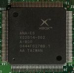
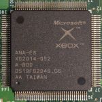
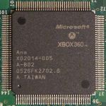
Engineering Samples by stepping.
B00
- Part Number: X02014-002
B02
- Part Number: X02014-005


