Y1 (GPU): Difference between revisions
No edit summary |
No edit summary |
||
| (60 intermediate revisions by 2 users not shown) | |||
| Line 3: | Line 3: | ||
| image = X02056-010.jpg | | image = X02056-010.jpg | ||
| image_size = 150px | | image_size = 150px | ||
| caption = X02056 | | caption = Original Y1 (X02056) | ||
| image2 = X817791-003.jpg | | image2 = X817791-003.jpg | ||
| image2_size = 150px | | image2_size = 150px | ||
| caption2 = X817791 | | caption2 = Revised Y1 (X817791) | ||
| partnumber = X02056<br>X817791 | | partnumber = X02056<br>X817791 | ||
| introduced = Late 2005 | | introduced = Late 2005 | ||
| designedby = ATi<br>Microsoft<br>NEC (eDRAM) | | designedby = ATi<br>Microsoft<br>NEC (eDRAM) | ||
| codename = | | codename = C1 | ||
| type = [[GPU]] | | type = [[GPU]] | ||
| usedin = [[Xenon (Motherboard)|Xenon]]<br>[[Zephyr#Zephyr_A|Zephyr_A]] | | usedin = [[Xenon (Motherboard)|Xenon]]<br>[[Zephyr#Zephyr_A|Zephyr_A]] | ||
| Line 17: | Line 17: | ||
| process = 90nm (Both dies) | | process = 90nm (Both dies) | ||
| package = Flip-chip BGA1017 | | package = Flip-chip BGA1017 | ||
| successor = [[Y2 (GPU)|Y2]] | | successor = [[Y2 (GPU)|Y2]]<br>[[Elpis (GPU)|Elpis]] | ||
}} | }} | ||
'''Y1''', | '''Y1''', codename '''C1''', is the launch model [[GPU]] and is used on the [[Xenon (Motherboard)|Xenon]] and [[Zephyr#Zephyr_A|Zephyr_A]] motherboards. Both dies are manufactured on a 90nm process. | ||
== Specifications == | == Specifications == | ||
=== GPU === | === GPU (Xenos C1) === | ||
{{GPU Specs}} | {{GPU Specs}} | ||
* A32 [[stepping]] | |||
* 90nm process | * 90nm process | ||
=== eDRAM === | === eDRAM (Edifis) === | ||
{{EDRAM Specs}} | {{EDRAM Specs}} | ||
* ES3 (C00) [[stepping]] | |||
* 90nm process | * 90nm process | ||
| Line 34: | Line 36: | ||
=== X02056 === | === X02056 === | ||
[[File:X02056-010-Korea.jpg|thumb|150px|upright|right|Korean X02056 from 2008]] | |||
[[File:X02056-012.jpg|thumb|150px|upright|right|Uncommon -012 model X02056 from 2005]] | |||
The initial version of the GPU Y1, used in the launch model consoles. It uses the [[Xenos C1]] [[GPU]] and [[Edifis]] [[eDRAM]]. {{Flip Chip Fault|t=overview}} | |||
* Part Number: X02056 (-010, -011, -012) | |||
* | |||
=== X817791 === | === X817791 === | ||
In Mid 2008, GPU Y1 received a revision and part number change. "GPU - Y1" markings were added to differentiate from other in-production chips. In addition, it uses a higher Tg underfill material and as a result, is known to be reliable. It is not known if there are any other differences. | |||
* Part Number: X817791 | * Part Number: X817791 | ||
* | |||
** {{ | == Prototypes == | ||
Engineering Samples by [[stepping]]. Text on many of these chips is very faint and hard to capture. Most use the older Xbox logo. | |||
=== A11/A11N1 === | |||
First version. Supposedly, the ES1 (A00) [[eDRAM]] is broken and does not work. | |||
* Part Numbers: | |||
** X02056-001 (A11) | |||
** X02056-002 (A11N1) | |||
[[File:X02056-001.jpg|150px]] | |||
[[File:X02056-002.jpg|150px]] | |||
=== A11N2 === | |||
Fixes the [[eDRAM]] issue with ES2 (B00). Two substrate colors have been seen. | |||
* Part Number: X02056-004 | |||
[[File:X02056-004.jpg|150px]] | |||
[[File:X02056-004-2.jpg|150px]] | |||
A debug substrate version also exists, marked as "GPU DBG". It is believed to have more debug traces. | |||
* Part Number: X02074-003 | |||
[[File:X02074-003.jpg|150px]] | |||
=== A21/A21N1 === | |||
Major update. Changed to ES3 (C00) [[eDRAM]]. Marked either A21 or A21N1, same silicon. A21N1 seen with a blue die. | |||
* Part Numbers: | |||
** X02056-006 (A21) | |||
** X02056-007 (A21N1) | |||
[[File:X02056-006.jpg|150px]] | |||
[[File:X02056-007.jpg|150px]] | |||
=== A21N2 === | |||
Very minor update. | |||
* Part Number: X02056-008 | |||
[[File:X02056-008.jpg|150px]] | |||
A debug substrate version also exists, marked as "GPU DBG". It is believed to have more debug traces. | |||
* Part Number: X02074-007 | |||
[[File:X02074-007.jpg|150px]] | |||
=== A31 === | |||
Major update. Also shown is a slow cornering chip with the final Xbox 360 logo. | |||
* Part Number: X02056-009 | |||
[[File:X02056-009.jpg|150px]] | |||
[[File:X02056-009-SS.jpg|150px]] | |||
=== A32 === | |||
Minor update. Engineering sample for the final production chip. | |||
* Part Number: X02056-010 (same as final) | |||
[[File:X02056-010-Early.jpg|150px]] | |||
{{Motherboard Components}} | |||
[[Category:Motherboard Components]] | |||
Latest revision as of 10:11, 12 September 2024
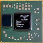
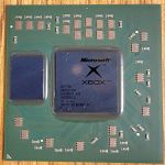
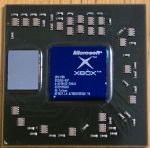
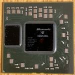
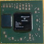 Original Y1 (X02056) | |
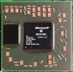
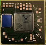
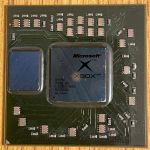
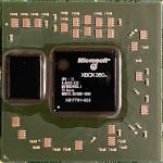 Revised Y1 (X817791) | |
| Part Number | X02056 X817791 |
|---|---|
| Introduced | Late 2005 |
| Designed By | ATi Microsoft NEC (eDRAM) |
| Codename | C1 |
| Type | GPU |
| Used In | Xenon Zephyr_A |
| Clock Speed | 500MHz |
| Memory | 10MB eDRAM |
| Process | 90nm (Both dies) |
| Package | Flip-chip BGA1017 |
| Successor | Y2 Elpis |
Y1, codename C1, is the launch model GPU and is used on the Xenon and Zephyr_A motherboards. Both dies are manufactured on a 90nm process.
Specifications
GPU (Xenos C1)
- 500Mhz clock speed
- 48 floating-point vector processors divided into 3 dynamically scheduled SIMD groups (16 each)
- Unified shader architecture
- 16 texture addressing units
- 16 texture filtering units
- 8 pixel rendering pipelines
- Direct access to CPU L2 cache
- A32 stepping
- 90nm process
eDRAM (Edifis)
- 10MB 256GB/s eDRAM
- Contains logic for:
- 4-sample anti-aliasing
- Alpha compositing
- Color
- Z/stencil buffering
- ES3 (C00) stepping
- 90nm process
Details
X02056
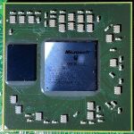
The initial version of the GPU Y1, used in the launch model consoles. It uses the Xenos C1 GPU and Edifis eDRAM. This chip contains a design defect in which low Tg underfill is used to support the bumps. This causes reliability issues and premature failure of the chip.
- Part Number: X02056 (-010, -011, -012)
X817791
In Mid 2008, GPU Y1 received a revision and part number change. "GPU - Y1" markings were added to differentiate from other in-production chips. In addition, it uses a higher Tg underfill material and as a result, is known to be reliable. It is not known if there are any other differences.
- Part Number: X817791
Prototypes
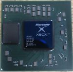
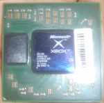
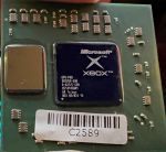
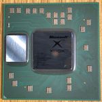
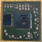
Engineering Samples by stepping. Text on many of these chips is very faint and hard to capture. Most use the older Xbox logo.
A11/A11N1
First version. Supposedly, the ES1 (A00) eDRAM is broken and does not work.
- Part Numbers:
- X02056-001 (A11)
- X02056-002 (A11N1)
A11N2
Fixes the eDRAM issue with ES2 (B00). Two substrate colors have been seen.
- Part Number: X02056-004
A debug substrate version also exists, marked as "GPU DBG". It is believed to have more debug traces.
- Part Number: X02074-003
A21/A21N1
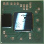
Major update. Changed to ES3 (C00) eDRAM. Marked either A21 or A21N1, same silicon. A21N1 seen with a blue die.
- Part Numbers:
- X02056-006 (A21)
- X02056-007 (A21N1)
A21N2
Very minor update.
- Part Number: X02056-008
A debug substrate version also exists, marked as "GPU DBG". It is believed to have more debug traces.
- Part Number: X02074-007
A31
Major update. Also shown is a slow cornering chip with the final Xbox 360 logo.
- Part Number: X02056-009
A32
Minor update. Engineering sample for the final production chip.
- Part Number: X02056-010 (same as final)
