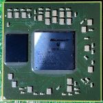
Y1 (GPU): Difference between revisions
No edit summary |
|||
| Line 73: | Line 73: | ||
=== A21/A21N1 === | === A21/A21N1 === | ||
Major update. Changed to ES3 (C00) [[eDRAM]]. Marked either A21 or A21N1, same silicon. | Major update. Changed to ES3 (C00) [[eDRAM]]. Marked either A21 or A21N1, same silicon. A21N1 seen with a blue die. | ||
* Part Numbers: | * Part Numbers: | ||
| Line 80: | Line 80: | ||
[[File:X02056-006.jpg|150px]] | [[File:X02056-006.jpg|150px]] | ||
[[File:X02056-007.jpg|150px]] | |||
=== A21N2 === | === A21N2 === | ||
Revision as of 14:18, 29 July 2024
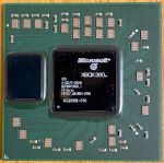
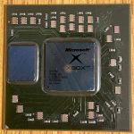
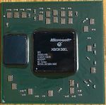 Original Y1 (X02056) | |
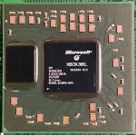
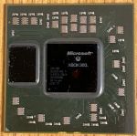
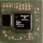 Revised Y1 (X817791) | |
| Part Number | X02056 X817791 |
|---|---|
| Introduced | Late 2005 |
| Designed By | ATi Microsoft NEC (eDRAM) |
| Codename | C1 |
| Type | GPU |
| Used In | Xenon Zephyr_A |
| Clock Speed | 500MHz |
| Memory | 10MB eDRAM |
| Process | 90nm (Both dies) |
| Package | Flip-chip BGA1017 |
| Successor | Y2 Elpis |
Y1, codename C1, is the launch model GPU and is used on the Xenon and Zephyr_A motherboards. Both dies are manufactured on a 90nm process.
Specifications
GPU
- 500Mhz clock speed
- 48 floating-point vector processors divided into 3 dynamically scheduled SIMD groups (16 each)
- Unified shader architecture
- 16 texture addressing units
- 16 texture filtering units
- 8 pixel rendering pipelines
- Direct access to CPU L2 cache
- A32 stepping
- 90nm process
eDRAM (Edifis)
- 10MB 256GB/s eDRAM
- Contains logic for:
- 4-sample anti-aliasing
- Alpha compositing
- Color
- Z/stencil buffering
- ES3 (C00) stepping
- 90nm process
Details
X02056
The initial version of the GPU Y1, used in the launch model consoles. It uses the Edifis eDRAM. This chip contains a design defect in which low Tg underfill is used to support the bumps. This causes reliability issues and premature failure of the chip.
- Part Number: X02056 (-010, -011, -012)
X817791
In Mid 2008, GPU Y1 received a revision and part number change. "GPU - Y1" markings were added to differentiate from other in-production chips. In addition, it uses a higher Tg underfill material and as a result, is known to be reliable. It is not known if there are any other differences.
- Part Number: X817791
Prototypes
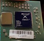
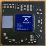
Engineering Samples by stepping. Text on many of these chips is very faint and hard to capture. Most use the older Xbox logo.
A11N1
First version. Supposedly, the ES1 (A00) eDRAM is broken and does not work.
- Part Number: X02056-002
A11N2
Fixes the eDRAM issue with ES2 (B00). Two substrate colors have been seen.
- Part Number: X02056-004
A debug substrate version also exists, marked as "GPU DBG". It is believed to have more debug traces.
- Part Number: X02074-003
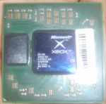
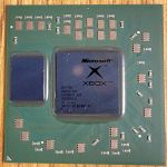
A21/A21N1
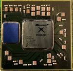
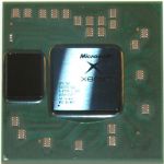
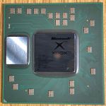
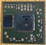
Major update. Changed to ES3 (C00) eDRAM. Marked either A21 or A21N1, same silicon. A21N1 seen with a blue die.
- Part Numbers:
- X02056-006 (A21)
- X02056-007 (A21N1)
A21N2
Very minor update.
- Part Number: X02056-008
A debug substrate version also exists, marked as "GPU DBG". It is believed to have more debug traces.
- Part Number: X02074-007
A31
Major update. Also shown is a slow cornering chip with the final Xbox 360 logo.
- Part Number: X02056-009
A32
Minor update. Engineering sample for the final production chip.
- Part Number: X02056-010 (same as final)
