Y2 (GPU): Difference between revisions
Jump to navigation
Jump to search
No edit summary |
No edit summary |
||
| Line 17: | Line 17: | ||
}} | }} | ||
'''Y2''' is an 80nm [[GPU]] and is used on the [[Zephyr#Zephyr_B|Zephyr_B]] motherboard. It is the successor to [[Y1 (GPU)|Y1]] | '''Y2''' is an 80nm [[GPU]] and is used on the [[Zephyr#Zephyr_B|Zephyr_B]] motherboard. It is the successor to [[Y1 (GPU)|Y1]]. Minimal changes were required to move from the 90nm to the 80nm process. The [[eDRAM]] was not shrunk and remains on a 90nm process. | ||
== Specifications == | == Specifications == | ||
=== GPU === | === GPU === | ||
{{GPU Specs}} | {{GPU Specs}} | ||
* B13L or B14L stepping | |||
* 80nm process | * 80nm process | ||
=== eDRAM === | === eDRAM === | ||
{{EDRAM Specs}} | {{EDRAM Specs}} | ||
* C00 stepping (with B13L) | |||
* ES3 stepping (with B14L) | |||
* 90nm process | * 90nm process | ||
| Line 32: | Line 35: | ||
[[File:X02127-006.jpg|thumb|150px|upright|right|A B14L Y2]] | [[File:X02127-006.jpg|thumb|150px|upright|right|A B14L Y2]] | ||
The PCIe ballout was de-swizzled (flipped) for the [[Zephyr#Zephyr_B|Zephyr_B]] motherboard, making this chip incompatible earlier motherboards. {{Flip Chip Fault|t=overview}} {{Flip Chip Fault|t=nofixed}} | The PCIe ballout was de-swizzled (flipped) for the [[Zephyr#Zephyr_B|Zephyr_B]] motherboard, making this chip incompatible earlier motherboards. B13L versions use the [[Edifis]] [[eDRAM]], while later B14L verions use the [[Styx]] eDRAM. {{Flip Chip Fault|t=overview}} {{Flip Chip Fault|t=nofixed}} | ||
* Part Number: X02127 | * Part Number: X02127 | ||
Revision as of 21:01, 14 June 2023
 | |
| Part Number | X02127 |
|---|---|
| Introduced | Early 2007 |
| Designed By | ATi Microsoft NEC (eDRAM) |
| Codename | C2 |
| Type | GPU |
| Used In | Zephyr_B |
| Clock Speed | 500MHz |
| Memory | 10MB eDRAM |
| Process | 80nm (GPU die) 90nm (eDRAM die) |
| Package | Flip-chip BGA1017 |
| Predecessor | Y1 |
| Successor | Rhea |
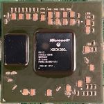
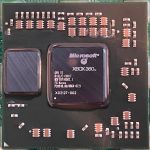
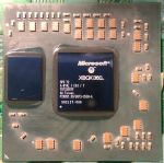
Y2 is an 80nm GPU and is used on the Zephyr_B motherboard. It is the successor to Y1. Minimal changes were required to move from the 90nm to the 80nm process. The eDRAM was not shrunk and remains on a 90nm process.
Specifications
GPU
- 500Mhz clock speed
- 48 floating-point vector processors divided into 3 dynamically scheduled SIMD groups (16 each)
- Unified shader architecture
- 16 texture addressing units
- 16 texture filtering units
- 8 pixel rendering pipelines
- Direct access to CPU L2 cache
- B13L or B14L stepping
- 80nm process
eDRAM
- 10MB 256GB/s eDRAM
- Contains logic for:
- 4-sample anti-aliasing
- Alpha compositing
- Color
- Z/stencil buffering
- C00 stepping (with B13L)
- ES3 stepping (with B14L)
- 90nm process
Details
The PCIe ballout was de-swizzled (flipped) for the Zephyr_B motherboard, making this chip incompatible earlier motherboards. B13L versions use the Edifis eDRAM, while later B14L verions use the Styx eDRAM. This chip contains a design defect in which low Tg underfill is used to support the bumps. This causes reliability issues and premature failure of the chip. No versions with higher Tg underfill were produced. Thus, no versions of this chip are known to be reliable.
- Part Number: X02127

