Oban: Difference between revisions
Jump to navigation
Jump to search
No edit summary |
|||
| (2 intermediate revisions by the same user not shown) | |||
| Line 19: | Line 19: | ||
}} | }} | ||
'''Oban''' is the final [[XCGPU]] and is used on the [[Winchester]] motherboard. It is the successor to [[ | '''Oban''' is the final [[XCGPU]] and is used on the [[Winchester]] motherboard. It is the successor to [[Vejle]] and is manufactured on the 32nm process. The chip combines the [[eDRAM]] into the CGPU die and thus the [[IHS|integrated heat spreader]] is no longer used. | ||
== Specifications == | == Specifications == | ||
=== CPU === | === CPU (Oban) === | ||
{{CPU Specs}} | {{CPU Specs}} | ||
* A03 [[stepping]] | * A03 [[stepping]] | ||
* 32nm process | * 32nm process | ||
=== GPU === | === GPU (Oban) === | ||
{{GPU Specs}} | {{GPU Specs}} | ||
* A03 [[stepping]] | * A03 [[stepping]] | ||
* 32nm process | * 32nm process | ||
=== eDRAM === | === eDRAM (Oban) === | ||
{{EDRAM Specs}} | {{EDRAM Specs}} | ||
* A03 [[stepping]] | * A03 [[stepping]] | ||
| Line 44: | Line 44: | ||
== Prototypes == | == Prototypes == | ||
Engineering Sample, stepping is unknown. | 2012 Engineering Sample, stepping is unknown. | ||
[[File:Oban-ES.jpg|150px]] | [[File:Oban-ES.jpg|150px]] | ||
Latest revision as of 00:36, 24 August 2024
 | |
| Part Number | X888839 X888841 |
|---|---|
| Introduced | Late 2014 |
| Designed By | IBM Microsoft |
| Type | XCGPU |
| Used In | Winchester |
| Clock Speed | 3.2GHz (CPU) 500MHz (GPU) |
| Cache | L1: 32KB/32KB (CPU) L2: 1MB (CPU) |
| Memory | 10MB eDRAM (GPU) |
| Instruction Set | PowerPC RISC (CPU) |
| Cores | 3 (CPU) |
| Threads | 6 (CPU) |
| Process | 32nm |
| Package | Flip-chip BGA899 |
| Predecessor | Vejle |
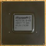
Oban is the final XCGPU and is used on the Winchester motherboard. It is the successor to Vejle and is manufactured on the 32nm process. The chip combines the eDRAM into the CGPU die and thus the integrated heat spreader is no longer used.
Specifications
CPU (Oban)
- 3 two-way SMD-capable RISC cores clocked at 3.2GHz
- SIMD: Two VMX128 units
- 32KB L1 data cache
- 32KB L1 instruction cache
- 1MB L2 cache at 1.6 GHz with a 256-bit bus
- 21.6GB/s FSB
- 768 bits of IBM eFUSE One-Time-Program memory for fusesets
- One-Time-Programmable ROM and 64KB SRAM for the 1BL and Config Ring
- Big-endian architecture
- A03 stepping
- 32nm process
GPU (Oban)
- 500Mhz clock speed
- 48 floating-point vector processors divided into 3 dynamically scheduled SIMD groups (16 each)
- Unified shader architecture
- 16 texture addressing units
- 16 texture filtering units
- 8 pixel rendering pipelines
- Direct access to CPU L2 cache
- A03 stepping
- 32nm process
eDRAM (Oban)
- 10MB 256GB/s eDRAM
- Contains logic for:
- 4-sample anti-aliasing
- Alpha compositing
- Color
- Z/stencil buffering
- A03 stepping
- 32nm process
Details
- Part Numbers:
- X888839
- X888841
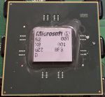
Prototypes
2012 Engineering Sample, stepping is unknown.
