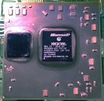
Zeus: Difference between revisions
No edit summary |
No edit summary |
||
| (41 intermediate revisions by 2 users not shown) | |||
| Line 9: | Line 9: | ||
| partnumber = X817793<br>X810478 | | partnumber = X817793<br>X810478 | ||
| introduced = Late 2008 | | introduced = Late 2008 | ||
| designedby = | | designedby = Microsoft | ||
| codename = | | codename = Y3 | ||
| type = [[GPU]] | | type = [[GPU]] | ||
| usedin = [[Jasper]] | | usedin = [[Jasper]] | ||
| clockspeed = 500MHz | | clockspeed = 500MHz | ||
| memory = 10MB [[eDRAM]] | | memory = 10MB [[eDRAM]] | ||
| process = 65nm (GPU die)<br> | | process = 65nm (GPU die)<br>90nm (eDRAM die) | ||
| package = Flip-chip BGA1017 | | package = Flip-chip BGA1017 | ||
| predecessor = [[Rhea (GPU)| | | predecessor = [[Rhea]]<br>[[Elpis (GPU)|Elpis]] | ||
| successor = [[ | | successor = [[Kronos]] | ||
}} | }} | ||
'''Zeus''', | '''Zeus''', codename '''Y3''', is a 65nm [[GPU]] and is used on the [[Jasper]] motherboard. It is the successor to [[Rhea]]. The 65nm process shrink required a redesign of the chip. The [[eDRAM]] was unchanged. Zeus was the first version of the [[GPU]] where all variants are known to be reliable. The 65nm redesign was done by Microsoft themselves, not ATi. | ||
== Specifications == | == Specifications == | ||
=== GPU === | === GPU (Gunga) === | ||
{{GPU Specs}} | {{GPU Specs}} | ||
* C22 [[stepping]] (X817793) | |||
* C23 [[stepping]] (X810478) | |||
* 65nm process | * 65nm process | ||
=== eDRAM === | === eDRAM (Styx-90) === | ||
{{EDRAM Specs}} | {{EDRAM Specs}} | ||
* | * FS21 [[stepping]] | ||
* 90nm process | |||
== Details == | == Details == | ||
All variants of Zeus use the [[Gunga]] [[GPU]] and [[Styx-90]] [[eDRAM]] | |||
=== X817793 === | === X817793 === | ||
The initial version of GPU Zeus | The initial version of GPU Zeus with C22 [[stepping]]. The ballout is compatible with the previous 90nm GPUs, however minor changes to the motherboard must be made. | ||
* Part Number: X817793 | * Part Number: X817793 | ||
=== X810478 === | === X810478 === | ||
A revised version of GPU Zeus | A revised version of GPU Zeus with C23 [[stepping]]. The specifics of what changed between the two cores is not known. This chip is a drop-in replacement for the earlier version of Zeus. | ||
* Part Number: X810478 | * Part Number: X810478 | ||
* | |||
== Prototypes == | |||
Engineering Samples by [[stepping]]. | |||
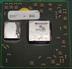
=== C11 === | |||
First version. | |||
[[File:X812419-001.jpg|150px]] | |||
* Part Number: X812419-001 | |||
=== C12 === | |||
Minor update. Marked as C12P. | |||
[[File:X813271-002.jpg|150px]] | |||
[[File:X813899-001.jpg|150px]] | |||
* Part Numbers: | |||
** X813271-002 | |||
** X813899-001 | |||
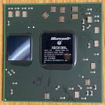
=== C21 === | |||
Major update. | |||
[[File:X815990-001.jpg|150px]] | |||
[[File:X815992-001.jpg|150px]] | |||
* Part Numbers: | |||
** X815990-001 | |||
** X815992-001 | |||
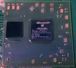
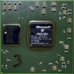
=== C22 === | |||
Minor update. Engineering sample for the final C22 production chip. | |||
[[File:X815988-002.jpg|150px]] | |||
[[File:X815989-002.jpg|150px]] | |||
[[File:X817124-001.jpg|150px]] | |||
[[File:X818063-001.jpg|150px]] | |||
* Part Numbers: | |||
** X815988-002 | |||
** X815989-002 | |||
** X817124-001 | |||
** X818063-001 | |||
=== C23 === | |||
Minor update. Engineering sample for the final C23 production chip. | |||
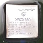
[[File:X819831-001.jpg|150px]] | |||
* Part Number: X819831-001 | |||
{{Motherboard Components}} | {{Motherboard Components}} | ||
[[Category:Motherboard Components]] | [[Category:Motherboard Components]] | ||
Latest revision as of 23:29, 23 August 2024
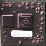
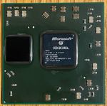 Original Zeus (X817793) | |
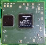
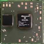 Revised Zeus (X810478) | |
| Part Number | X817793 X810478 |
|---|---|
| Introduced | Late 2008 |
| Designed By | Microsoft |
| Codename | Y3 |
| Type | GPU |
| Used In | Jasper |
| Clock Speed | 500MHz |
| Memory | 10MB eDRAM |
| Process | 65nm (GPU die) 90nm (eDRAM die) |
| Package | Flip-chip BGA1017 |
| Predecessor | Rhea Elpis |
| Successor | Kronos |
Zeus, codename Y3, is a 65nm GPU and is used on the Jasper motherboard. It is the successor to Rhea. The 65nm process shrink required a redesign of the chip. The eDRAM was unchanged. Zeus was the first version of the GPU where all variants are known to be reliable. The 65nm redesign was done by Microsoft themselves, not ATi.
Specifications
GPU (Gunga)
- 500Mhz clock speed
- 48 floating-point vector processors divided into 3 dynamically scheduled SIMD groups (16 each)
- Unified shader architecture
- 16 texture addressing units
- 16 texture filtering units
- 8 pixel rendering pipelines
- Direct access to CPU L2 cache
- C22 stepping (X817793)
- C23 stepping (X810478)
- 65nm process
eDRAM (Styx-90)
- 10MB 256GB/s eDRAM
- Contains logic for:
- 4-sample anti-aliasing
- Alpha compositing
- Color
- Z/stencil buffering
- FS21 stepping
- 90nm process
Details
All variants of Zeus use the Gunga GPU and Styx-90 eDRAM
X817793
The initial version of GPU Zeus with C22 stepping. The ballout is compatible with the previous 90nm GPUs, however minor changes to the motherboard must be made.
- Part Number: X817793
X810478
A revised version of GPU Zeus with C23 stepping. The specifics of what changed between the two cores is not known. This chip is a drop-in replacement for the earlier version of Zeus.
- Part Number: X810478
Prototypes
Engineering Samples by stepping.
C11
First version.
- Part Number: X812419-001
C12
Minor update. Marked as C12P.
- Part Numbers:
- X813271-002
- X813899-001
C21
Major update.
- Part Numbers:
- X815990-001
- X815992-001
C22
Minor update. Engineering sample for the final C22 production chip.
- Part Numbers:
- X815988-002
- X815989-002
- X817124-001
- X818063-001
C23
Minor update. Engineering sample for the final C23 production chip.
- Part Number: X819831-001
