Venus: Difference between revisions
Jump to navigation
Jump to search
No edit summary |
No edit summary |
||
| Line 11: | Line 11: | ||
| process = 90nm (GPU die)<br>80nm (eDRAM die) | | process = 90nm (GPU die)<br>80nm (eDRAM die) | ||
| package = Flip-chip BGA1017 | | package = Flip-chip BGA1017 | ||
| successor = [[Rhea]] | |||
}} | }} | ||
Revision as of 12:19, 12 February 2024
 | |
| Part Number | X809141 |
|---|---|
| Introduced | Early 2006 |
| Designed By | ATi Microsoft NEC (eDRAM) |
| Type | GPU |
| Clock Speed | 500MHz |
| Memory | 10MB eDRAM |
| Process | 90nm (GPU die) 80nm (eDRAM die) |
| Package | Flip-chip BGA1017 |
| Successor | Rhea |
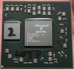
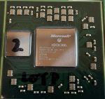
Venus is an engineering sample GPU used to checkout the first version of the 80nm Styx eDRAM. The GPU die is the same 90nm die as Y1.
Specifications
GPU
- 500Mhz clock speed
- 48 floating-point vector processors divided into 3 dynamically scheduled SIMD groups (16 each)
- Unified shader architecture
- 16 texture addressing units
- 16 texture filtering units
- 8 pixel rendering pipelines
- Direct access to CPU L2 cache
- A32 stepping
- 90nm process
eDRAM
- 10MB 256GB/s eDRAM
- Contains logic for:
- 4-sample anti-aliasing
- Alpha compositing
- Color
- Z/stencil buffering
- FS11 stepping
- 80nm process
Details
Based on the manufacturing date, it is speculated that this chip was designed in order to test Styx-80 before the Y2 or Y3 GPU dies were available. The GPU die is marked with "GPU Y3/Venus ES", indicating that it is part of the Y3 program. Little else is known about Venus.
