Venus: Difference between revisions
Jump to navigation
Jump to search
No edit summary |
No edit summary |
||
| Line 13: | Line 13: | ||
}} | }} | ||
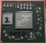
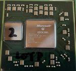
'''Venus''' is an engineering sample [[GPU]] used to checkout the first version of the 80nm [[Styx]] eDRAM. The GPU die is the same 90nm die as [[Y1 (GPU)|Y1]]. | '''Venus''' is an engineering sample [[GPU]] used to checkout the first version of the 80nm [[Styx]] eDRAM. The GPU die is the same 90nm die as [[Y1 (GPU)|Y1]], but marked with "GPU Y3/Venus ES". | ||
== Specifications == | == Specifications == | ||
Revision as of 16:10, 8 February 2024
 | |
| Part Number | X809141 |
|---|---|
| Introduced | Early 2006 |
| Designed By | ATi Microsoft NEC (eDRAM) |
| Type | GPU |
| Clock Speed | 500MHz |
| Memory | 10MB eDRAM |
| Process | 90nm (GPU die) 80nm (eDRAM die) |
| Package | Flip-chip BGA1017 |
Venus is an engineering sample GPU used to checkout the first version of the 80nm Styx eDRAM. The GPU die is the same 90nm die as Y1, but marked with "GPU Y3/Venus ES".
Specifications
GPU
- 500Mhz clock speed
- 48 floating-point vector processors divided into 3 dynamically scheduled SIMD groups (16 each)
- Unified shader architecture
- 16 texture addressing units
- 16 texture filtering units
- 8 pixel rendering pipelines
- Direct access to CPU L2 cache
- A32 stepping
- 90nm process
eDRAM
- 10MB 256GB/s eDRAM
- Contains logic for:
- 4-sample anti-aliasing
- Alpha compositing
- Color
- Z/stencil buffering
- FS11 stepping
- 80nm process
Details
Based on the manufacturing date, it is speculated that this chip was designed in order to test Styx-80 before the Y2 or Gunga (Y3) GPU dies were available. Little else is known about Venus.
