Themis: Difference between revisions
Jump to navigation
Jump to search
No edit summary |
|||
| Line 23: | Line 23: | ||
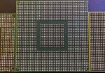
[[File:X816343-002-bga.jpg|thumb|150px|upright|right|Themis' BGA compared to a regular [[GPU]] (left) and [[XCGPU]] (right)]] | [[File:X816343-002-bga.jpg|thumb|150px|upright|right|Themis' BGA compared to a regular [[GPU]] (left) and [[XCGPU]] (right)]] | ||
Little is known about Themis. The BGA layout is absolutely massive. The die etchings mention the Styx-90 stepping FS21, but it is not included on the package. The reason for this is unknown. | Little is known about Themis. The BGA layout is absolutely massive. The die etchings mention the [[Styx]]-90 stepping FS21, but it is not included on the package. The reason for this is unknown. | ||
* Part Number: X816343 | * Part Number: X816343 | ||
Revision as of 05:29, 5 April 2024
 | |
| Part Number | X816343 |
|---|---|
| Introduced | Early 2008 |
| Designed By | Microsoft |
| Type | GPU |
| Clock Speed | 500MHz |
| Process | 65nm (GPU die) |
| Package | Unknown |
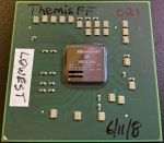
Themis is an engineering sample GPU likely created to evaluate final Gunga silicon.
Specifications
GPU
- 500Mhz clock speed
- 48 floating-point vector processors divided into 3 dynamically scheduled SIMD groups (16 each)
- Unified shader architecture
- 16 texture addressing units
- 16 texture filtering units
- 8 pixel rendering pipelines
- Direct access to CPU L2 cache
- C22 stepping
- 65nm process
Details
Little is known about Themis. The BGA layout is absolutely massive. The die etchings mention the Styx-90 stepping FS21, but it is not included on the package. The reason for this is unknown.
- Part Number: X816343
